WR-03 Low Power Termination
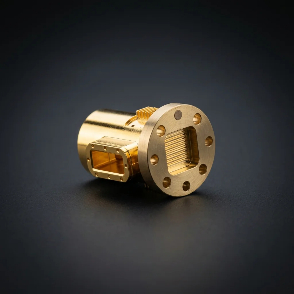
The WR-03 Low Power Termination is a precision-engineered waveguide component that provides an exact precision match for terminating unused ports during VNA calibration and testing. It is specifically designed for the 220 - 330 GHz frequency range, serving as a critical building block in J-Band infrastructure.
Low-power terminations prioritize absolute minimum VSWR over heat dissipation, using a highly engineered, delicate absorbing element designed for milliwatt-level measurement accuracy. Operating in the extreme J-Band (220-330 GHz), WR-03 is the absolute cutting edge of commercial waveguide technology. The 0.034" x 0.017" aperture is thinner than a credit card, requiring flawless electroforming.
Key Features
Compact Form Factor
Designed for bench-top and rack-mounted test setups where space and weight are critical considerations.
Precision Matched Load
Engineered for excellent return loss and VSWR performance across the full operating frequency band.
Laboratory Grade
Meets the exacting standards required for network analyzer calibration and precision RF measurements.
Corrosion Resistant
Gold-plated finish provides long-term environmental durability and consistent electrical performance.
J-Band Use Cases
ALMA Telescope
Sub-millimeter astronomy
THz Spectroscopy
Molecular rotational sensing
Material Science
Dielectric characterization
Medical Imaging
Non-ionizing THz scanners
More Low Power Terminations
Frequently Asked Questions
Can a low power termination be used for calibration?+
Yes. Low power terminations are frequently used as the "Load" standard during a Short-Short-Load-Thru (SSLT) calibration on a Vector Network Analyzer, requiring them to have near-perfect return loss (better than 30 dB).
What is the physical size of the WR-03 opening?+
The internal hole of a WR-03 waveguide is 0.034 inches by 0.017 inches (0.86 mm by 0.43 mm). It is so small that a standard mechanical pencil lead cannot fit inside it. Dust particles alone can severely ruin the VSWR.
Why is gold plating mandatory on WR-03?+
At 300 GHz, the skin depth of the RF signal is less than 0.1 micrometers. The signal travels exclusively on the very outer layer of atoms on the waveguide wall. Even a microscopic layer of copper oxidation will completely absorb the terahertz wave, making non-oxidizing gold plating absolutely mandatory.