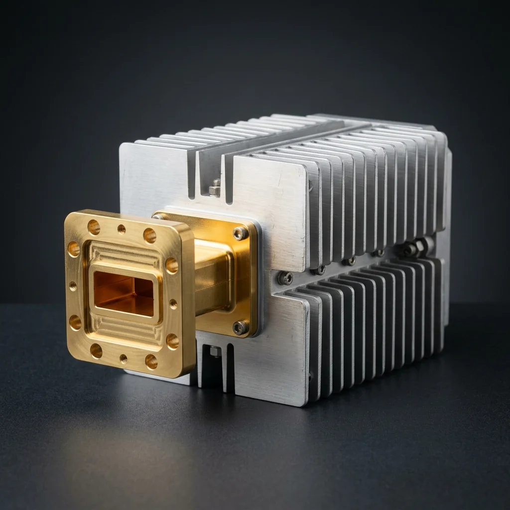
WR-03 High Power Termination
The WR-03 High Power Termination is a precision-engineered waveguide component that absorbs massive amounts of RF energy, safely dissipating it as heat to prevent signal reflection. It is specifically designed for the 220 - 330 GHz frequency range, serving as a critical building block in J-Band infrastructure.
High-power terminations feature a wedge-shaped ceramic or silicon-carbide absorbing element bonded to a large external heatsink with cooling fins to maximize thermal convection. Operating in the extreme J-Band (220-330 GHz), WR-03 is the absolute cutting edge of commercial waveguide technology. The 0.034" x 0.017" aperture is thinner than a credit card, requiring flawless electroforming.
Key Features
High Power Capacity
Rated for sustained high-power RF absorption with integrated thermal management for reliable operation.
Heat Dissipation
Cooling fin heatsink design provides maximum thermal dissipation for continuous high-power operation.
Rugged Construction
Heavy-duty OFHC copper body engineered for demanding transmitter test and system burn-in environments.
Full-Band Coverage
Maintains excellent VSWR and return loss across the complete operating bandwidth even at elevated power levels.
J-Band Use Cases
ALMA Telescope
Sub-millimeter astronomy
THz Spectroscopy
Molecular rotational sensing
Material Science
Dielectric characterization
Medical Imaging
Non-ionizing THz scanners
More High Power Terminations
Frequently Asked Questions
What happens if a high power termination overheats?+
If the absorbing wedge exceeds its thermal limit, it can crack or outgas. More importantly, as it heats up, its electrical resistance changes, ruining the impedance match and causing massive RF reflections (high VSWR) back into your amplifier.
What is the physical size of the WR-03 opening?+
The internal hole of a WR-03 waveguide is 0.034 inches by 0.017 inches (0.86 mm by 0.43 mm). It is so small that a standard mechanical pencil lead cannot fit inside it. Dust particles alone can severely ruin the VSWR.
Why is gold plating mandatory on WR-03?+
At 300 GHz, the skin depth of the RF signal is less than 0.1 micrometers. The signal travels exclusively on the very outer layer of atoms on the waveguide wall. Even a microscopic layer of copper oxidation will completely absorb the terahertz wave, making non-oxidizing gold plating absolutely mandatory.