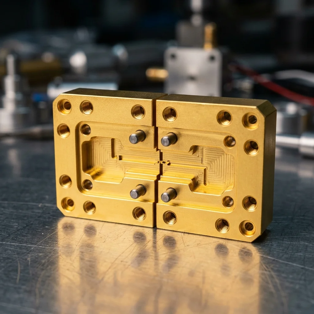
At frequencies below 100 GHz, waveguide manufacturing is a mature process. Standard CNC milling machines cut rectangular channels into solid metal blocks, and the resulting waveguides deliver predictable performance with well-understood tolerances. Above 100 GHz, the game changes. WR-10 waveguide for the 75 to 110 GHz W-band has an aperture of 2.54 mm by 1.27 mm. WR-03 for 220 to 325 GHz shrinks to 0.864 mm by 0.432 mm. At WR-1.5 for 500 to 750 GHz, the aperture is 0.381 mm by 0.191 mm, smaller than the tip of a ballpoint pen. Machining a rectangular hole this small with the surface finish and dimensional accuracy required for low-loss waveguide transmission is beyond the capability of conventional end mills. Split-block construction is the manufacturing technique that makes sub-THz waveguide possible.
The Split-Block Concept
Instead of machining a complete rectangular waveguide channel into a single block (which requires plunging an end mill into a narrow slot with a depth-to-width aspect ratio of 2:1 or greater), the split-block approach divides the waveguide along a symmetry plane and machines each half-channel into a separate metal block. The two halves are then aligned using precision dowel pins and bolted together, forming the complete waveguide channel at the junction.
Two splitting planes are possible. An E-plane split divides the waveguide along the broad wall, cutting the guide height in half. Each block contains a shallow channel that is one half of the full aperture height (b/2) and the full aperture width (a). An H-plane split divides along the narrow wall, cutting the guide width in half. Each block contains a channel that is the full height (b) but half the width (a/2). The choice between E-plane and H-plane splitting has significant manufacturing and RF performance implications.
| Waveguide | Frequency (GHz) | Aperture (mm) | Wall Tolerance | Surface Finish | Typical Loss (dB/cm) |
|---|---|---|---|---|---|
| WR-10 | 75 to 110 | 2.540 × 1.270 | ± 5 μm | 0.4 μm Ra | 0.03 to 0.05 |
| WR-06 | 110 to 170 | 1.651 × 0.826 | ± 3 μm | 0.3 μm Ra | 0.05 to 0.08 |
| WR-03 | 220 to 325 | 0.864 × 0.432 | ± 2 μm | 0.2 μm Ra | 0.10 to 0.20 |
| WR-1.5 | 500 to 750 | 0.381 × 0.191 | ± 1 μm | 0.1 μm Ra | 0.30 to 0.60 |
| WR-1.0 | 750 to 1100 | 0.254 × 0.127 | ± 0.5 μm | 0.05 μm Ra | 0.50 to 1.20 |
E-Plane vs. H-Plane Splitting
The E-plane split is the more common choice for sub-THz waveguide because the machining geometry is more favorable. Each half-block requires a shallow, wide channel (full width a, half height b/2) that can be cut with a standard flat-bottom end mill. The aspect ratio of the channel is approximately 3:1 (width to depth), well within the capability of micro end mills down to 0.1 mm diameter. The critical dimension is the depth of each half-channel; when the two halves are assembled, the total depth must equal the specified waveguide height b within the tolerance budget.
The RF consequence of an E-plane split is a seam running along the center of the broad wall, perpendicular to the TE10 mode's electric field. If the two halves do not mate perfectly, a gap at the seam allows current to flow across the discontinuity, increasing conductor loss and potentially radiating energy from the waveguide. The current density on the broad wall peaks at the center (exactly where the seam is), making the E-plane split particularly sensitive to gap quality. Contact resistance across the seam must be minimized through surface finish, clamping force, and plating.
The H-plane split places the seam along the narrow wall, where the TE10 mode's wall current is zero in the ideal case. This means that a small gap at the seam produces negligible additional loss or radiation, making the H-plane split inherently more forgiving of alignment errors. However, the machining is more difficult: each half-block requires a deep, narrow channel (full height b, half width a/2) with a 1:2 aspect ratio (width to depth). At WR-03, this means cutting a 0.432 mm deep channel that is only 0.432 mm wide, requiring micro end mills with extreme aspect ratios and slow, careful machining to prevent tool deflection.
CNC Micro-Machining at Sub-THz Tolerances
The dimensional tolerances for sub-THz waveguide are measured in micrometers. At WR-03, the waveguide width must be held to ± 2 μm to maintain the cutoff frequency within acceptable limits. A 2 μm error in the broad dimension shifts the cutoff frequency by approximately 0.5 GHz, which is tolerable. A 10 μm error shifts the cutoff by 2.5 GHz and can push the operating band uncomfortably close to the cutoff, increasing dispersion and loss.
Dimensional Tolerance and Cutoff Frequency: For a rectangular waveguide, fc = c / (2a), where a = broad dimension. At WR-03, a = 0.864 mm, fc = 173.6 GHz. A ±2 μm tolerance on a shifts fc by ±0.4 GHz (0.23%). At WR-1.0, a = 0.254 mm, fc = 590 GHz; the same ±2 μm tolerance shifts fc by ±4.6 GHz (0.78%), which can push the lower operating frequency below cutoff. This is why WR-1.0 and smaller require ±0.5 μm tolerances, at the limit of commercial CNC capability.
Modern 5-axis CNC micro-milling machines with linear motor drives and glass-scale encoders achieve positioning accuracy of ± 1 μm and repeatability of ± 0.5 μm. Spindle speeds of 40,000 to 80,000 RPM are used with carbide or diamond-coated micro end mills ranging from 0.05 to 0.5 mm diameter. Tool wear is a constant concern: a 0.1 mm end mill machining tellurium copper can wear 2 to 5 μm in diameter over a single block, changing the channel width partway through the cut. Tool wear compensation in the CNC controller and frequent tool changes (every 10 to 20 minutes of cutting) mitigate this effect.
The block material is typically tellurium copper (CDA 145) for its excellent machinability and high conductivity, or aluminum 6061-T6 for lower-frequency bands where the larger dimensions are more forgiving. At RF Essentials, our waveguide product line from WR-03 through WR-430 is manufactured on precision CNC equipment calibrated to maintain these sub-micrometer tolerances across production runs.
Surface Finish and Plating
Surface roughness directly affects waveguide loss at sub-THz frequencies because the skin depth decreases with frequency. At 300 GHz, the skin depth in copper is approximately 0.12 μm. If the surface roughness (Ra) approaches or exceeds the skin depth, the effective conductor path length increases as the current follows the rough surface contour, increasing the resistive loss. The Hammerstad-Jensen model estimates the roughness correction factor: at Ra = 0.2 μm (8 μin), the loss increase is approximately 30% above the smooth-wall theoretical value. At Ra = 0.5 μm, the increase exceeds 60%.
Achieving 0.1 to 0.2 μm Ra surface finish inside a 0.4 mm wide channel requires specialized machining strategies: light finishing passes with sharp tools, optimized feed rates, and sometimes post-machining polishing with diamond-loaded abrasive compounds. Electroplating with gold (over a nickel barrier layer) adds 1 to 5 μm of gold, which improves corrosion resistance and provides a consistent, low-resistance surface. The plating must be uniform and must not build up excessively in corners, which would change the waveguide cross-section geometry.
Block Alignment and Assembly
The two halves of a split-block waveguide are aligned using precision dowel pins inserted into reamed holes in both blocks. The pin diameter tolerance is ± 1 μm, and the hole positions are machined in the same setup as the waveguide channel to ensure registration. When the blocks are bolted together, the dowel pins constrain the relative position of the two half-channels to within the pin-to-hole clearance, typically 1 to 3 μm.
Clamping force must be sufficient to close the seam completely without distorting the block. For a tellurium copper block measuring 25 mm by 25 mm by 10 mm, the bolt torque is typically 3 to 5 inch-pounds on 2-56 or 4-40 stainless steel screws. The block surfaces in contact are lapped flat to within 0.5 μm (optical flat quality) to ensure metal-to-metal contact across the entire seam area.
Verification of the assembled split-block is performed by measuring insertion loss and return loss across the operating band. A well-made WR-03 split-block straight section exhibits insertion loss of 0.10 to 0.15 dB/cm and return loss better than 25 dB across the 220 to 325 GHz band. If the seam is not properly closed, the return loss degrades (below 20 dB) and the insertion loss increases, particularly at the upper end of the band where the wavelength is shortest and most sensitive to discontinuities. Our engineering team at RF Essentials uses precision waveguide terminations as reference loads during split-block verification to ensure the measurement setup does not contribute systematic errors to the component characterization.
Split-block construction is the enabling manufacturing technique for the sub-THz revolution in communications, sensing, and spectroscopy. As 6G research pushes toward the D-band (110 to 170 GHz) and beyond, and as terahertz imaging systems move from laboratory demonstrations to field-deployable instruments, the demand for precision split-block waveguide grows. The manufacturers who can hold micrometer tolerances, achieve sub-micrometer surface finishes, and align split-block halves with optical precision will define what is possible at the upper frontier of the microwave spectrum.
RF Essentials manufactures precision waveguide components from WR-03 (220 to 325 GHz) through WR-430 (1.7 to 2.6 GHz). Our sub-THz products are CNC machined from tellurium copper with gold plating and ship with measured S-parameter data.
Frequently Asked Questions
Why is split-block construction needed for sub-terahertz waveguide?
Above 100 GHz the apertures become tiny, with WR-1.5 measuring just 0.381 by 0.191 mm, and machining a rectangular channel that small with the required surface finish and accuracy is beyond a conventional end mill plunging a 2 to 1 slot. Split-block construction divides the waveguide along a symmetry plane, machines each half-channel into a separate metal block, then aligns the halves with precision dowel pins and bolts them together to form the full channel.
What is the difference between E-plane and H-plane split blocks?
An E-plane split divides along the broad wall into shallow, wide half-channels that are easy to machine with a flat end mill, but the seam falls where the broad-wall current peaks, so any gap raises loss and can radiate. An H-plane split divides along the narrow wall, where the wall current is ideally zero, so it forgives alignment errors, but each half needs a deep, narrow channel that is much harder to cut. E-plane is the more common choice.
How tight do dimensional tolerances get for sub-terahertz waveguide?
Very tight. At WR-03 the broad dimension must hold to 2 micrometers, which shifts the cutoff frequency only about 0.4 GHz, but at WR-1.0 that same 2 micrometers shifts cutoff by 4.6 GHz and could push the lower band edge below cutoff, so WR-1.0 requires 0.5 micrometer tolerances at the very limit of commercial CNC. Five-axis micro-milling with glass-scale encoders reaches about 1 micrometer positioning, and micro end-mill tool wear is a constant concern.