For three decades, gallium arsenide (GaAs) was the undisputed king of microwave semiconductors. Every military radar, every satellite transponder, and every cellular base station power amplifier ran on GaAs. It was the material that made the microwave industry possible. And now it is being systematically replaced by gallium nitride (GaN) across nearly every high-performance RF application.
This is not a gradual transition. It is a generational shift driven by physics, funded by defense budgets, and accelerated by commercial demand for higher power density, wider bandwidth, and better thermal performance. If you are specifying power amplifiers, TR modules, or solid-state transmitters for any application above 1 GHz, GaN is almost certainly the right choice today. Understanding why requires looking at the material properties that make GaN fundamentally superior for high-power RF.
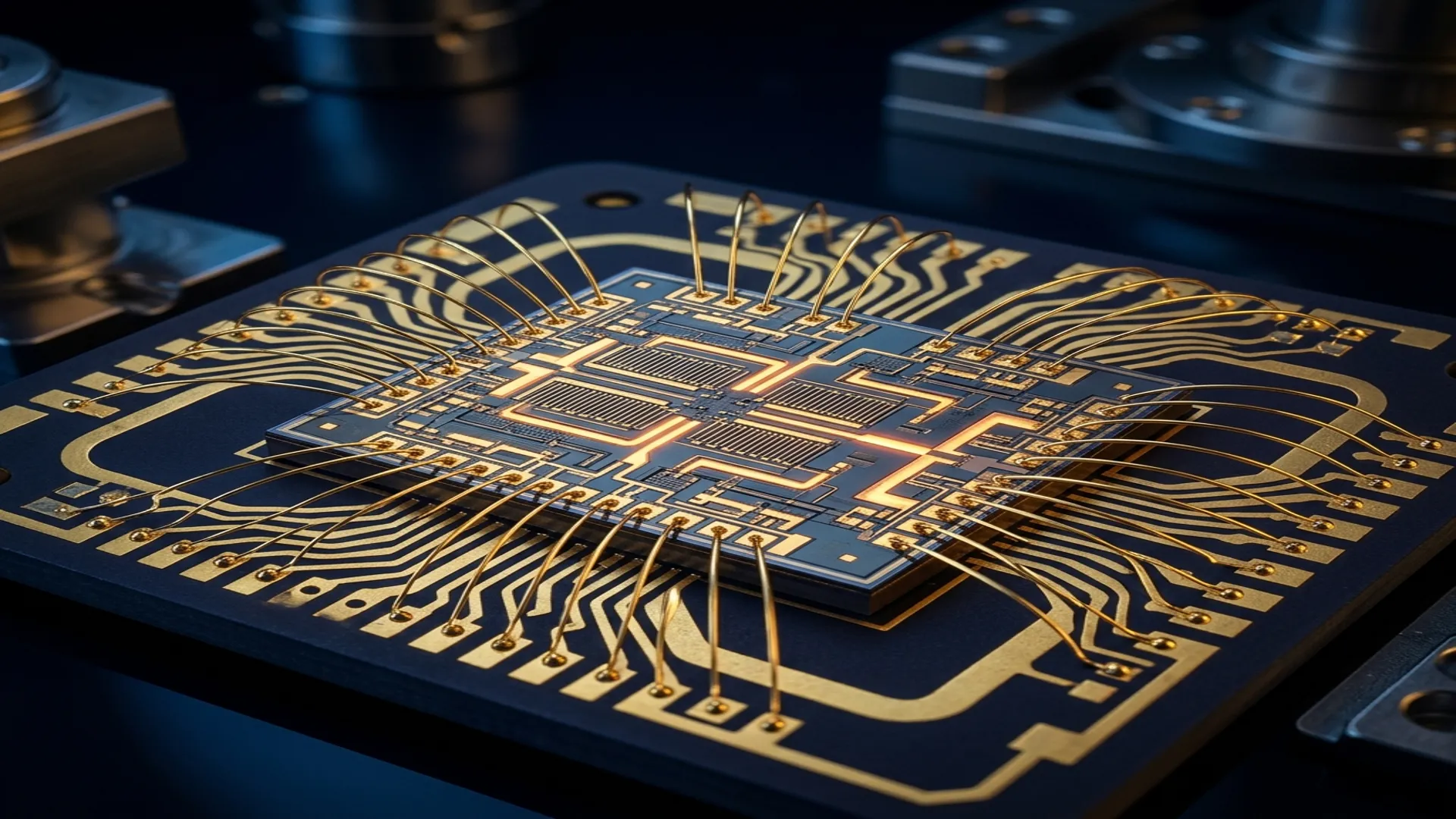
1. The Material Physics: Why GaN Wins
The performance advantages of GaN over GaAs are not incremental improvements. They are order-of-magnitude differences in the material properties that matter most for power amplifier design.
| Property | GaAs | GaN (on SiC) | Advantage Factor |
|---|---|---|---|
| Bandgap (eV) | 1.42 | 3.40 | 2.4× |
| Breakdown field (MV/cm) | 0.4 | 3.3 | 8× |
| Electron saturation velocity (cm/s) | 1.0 × 10⁷ | 2.5 × 10⁷ | 2.5× |
| Thermal conductivity of substrate (W/m·K) | 46 (GaAs) | 490 (SiC) | 10× |
| Typical power density (W/mm) | 0.5 to 1.5 | 5 to 10 | 5 to 10× |
| Max operating voltage (V) | 10 to 15 | 28 to 50 | 3 to 5× |
The 3.4 eV bandgap of GaN is the foundation of everything else. A wider bandgap means the material can sustain higher electric fields before breakdown, which means higher operating voltages, which means higher output power from a given device area. A GaN HEMT operating at 28V delivers the same output power as a GaAs device operating at 10V with roughly one-third the current, which simplifies the power supply and reduces I²R losses.
The power density advantage is the specification that matters most at the system level. A GaAs amplifier producing 100W at X-band might require a die area of 100 mm². The equivalent GaN device achieves the same 100W from a die area of 10 to 20 mm². That 5 to 10× reduction in die area directly translates to smaller modules, lighter subsystems, and more elements per unit area in a phased array.
The SiC Substrate: GaN's thermal advantage comes as much from its substrate as from the semiconductor itself. GaN grown on silicon carbide (SiC) benefits from SiC's thermal conductivity of 490 W/m·K, which is over 10 times higher than GaAs. This means heat generated in the GaN transistor channel is conducted away to the heatsink much more efficiently, allowing the device to operate at higher power densities without exceeding junction temperature limits. GaN-on-Si is cheaper but thermally inferior (silicon thermal conductivity is 150 W/m·K), making it suitable for lower-power commercial applications but not for high-power military radar.
2. The Defense Programs Driving Adoption
GaN's transition from lab curiosity to production technology was funded almost entirely by the U.S. Department of Defense. The DARPA Wide Bandgap Semiconductor (WBGS) program, launched in 2002, and its successor programs invested over $500 million in GaN device technology, foundry qualification, and reliability testing over two decades. That investment has paid off.
AESA Radar
Every new-generation AESA radar under development or in production uses GaN TR modules. The AN/APG-83 SABR (Scalable Agile Beam Radar) for F-16, the AN/APG-85 for F-35 Block 4, the AN/SPY-6(V) for the Navy's DDG(X) and constellation-class frigates, and the LTAMDS (Lower Tier Air and Missile Defense Sensor) for the Army all use GaN-based TR modules. The higher power per element means fewer elements are needed for the same effective radiated power, or the same number of elements delivers significantly greater detection range.
Electronic Warfare
EW jammers require broadband, high-power amplifiers that can cover multiple octaves of bandwidth. GaN's inherent wideband capability (a consequence of its high electron velocity and low parasitic capacitance) makes it the natural choice. The Next Generation Jammer (NGJ) on the EA-18G Growler uses GaN power amplifiers to deliver wideband jamming power across a broader frequency range than GaAs-based predecessors.
Satellite Communications
GaN is displacing traveling wave tubes (TWTs) in satellite transponders, a market TWTs dominated for 60 years. GaN solid-state power amplifiers (SSPAs) offer lower mass per watt, no warm-up time, graceful degradation (a single transistor failure does not kill the amplifier), and longer operational lifetimes than TWTs. For ground segment BUCs and HPAs, GaN enables higher power output in smaller, lighter, more field-serviceable packages.
3. The Commercial Crossover
GaN is no longer a defense-only technology. Commercial adoption is accelerating in several high-volume markets:
- 5G base station power amplifiers: The massive MIMO antennas used in 5G base stations (64 to 256 elements) require compact, efficient power amplifiers at each element. GaN-on-SiC dominates the sub-6 GHz 5G PA market, with suppliers like Wolfspeed, Qorvo, and MACOM shipping millions of units annually.
- Cable/broadband infrastructure: DOCSIS 4.0 cable amplifiers are transitioning from GaAs to GaN to achieve the higher output power and linearity required for full-duplex operation.
- Industrial and scientific: GaN amplifiers are replacing magnetrons and klystrons in medical linear accelerators, industrial heating, and particle accelerator RF systems.
4. What GaN Cannot Do (Yet)
| Limitation | Current Status | Impact |
|---|---|---|
| Low-noise amplifiers | GaN NF is 1.0 to 1.5 dB at X-band vs. 0.3 to 0.5 dB for GaAs/InP | GaAs and InP still dominate LNA applications where noise figure is critical |
| Cost at low volumes | GaN-on-SiC wafers cost 3 to 5× more than GaAs wafers | Uneconomical for low-power, cost-sensitive consumer applications |
| Frequency above 100 GHz | InP HEMT outperforms GaN above W-band | InP remains the choice for 100+ GHz systems and THz applications |
| Reliability data maturity | GaN MTTF data is 10 to 15 years old vs. 30+ years for GaAs | Some long-life satellite programs still specify GaAs for heritage reliability |
5. What This Means for the RF Hardware Stack
GaN changes the amplifier. But the waveguide, the termination, the coupler, and the circulator feeding that amplifier still need to handle the power. In fact, GaN's higher power densities place greater demands on the passive component chain. A GaN PA producing 200W in a Ka-band AESA module requires waveguide power dividers, combiners, and terminations rated for higher average and peak power levels than their GaAs-era predecessors. Thermal management of the passive chain becomes more critical because the heat generated by a GaN PA is concentrated in a smaller area.
For system integrators, the GaN transition is not just a semiconductor swap. It is a re-evaluation of the entire signal path, from power supply to antenna aperture. The components downstream of the PA must be designed, specified, and tested for the new power and thermal environment that GaN creates.
RF Essentials manufactures precision waveguide components, high-power terminations, and integrated assemblies rated for the power densities that GaN-based systems demand. All products are made in the USA.
Frequently Asked Questions
Why is gallium nitride replacing gallium arsenide in high-power RF?
GaN's 3.4 eV bandgap, against 1.42 eV for GaAs, sustains roughly eight times the breakdown field, which allows 28 to 50 V operation and power densities of 5 to 10 W per millimeter versus 0.5 to 1.5 for GaAs. A GaN device produces the same 100 W from a 10 to 20 square millimeter die that GaAs needs 100 square millimeters for. That smaller die shrinks modules and packs more elements into a phased array.
Why is GaN grown on a silicon carbide substrate?
Much of GaN's thermal advantage comes from the substrate. Silicon carbide conducts heat at about 490 W per meter-kelvin, more than ten times GaAs, so heat generated in the transistor channel reaches the heat sink efficiently and the device can run at high power density without exceeding its junction temperature limit. GaN-on-silicon is cheaper but thermally inferior at 150 W per meter-kelvin, which suits lower-power commercial parts rather than high-power radar.
Where do GaAs and InP still beat GaN?
Low-noise amplifiers. GaN noise figure is about 1.0 to 1.5 dB at X-band, while GaAs and InP reach 0.3 to 0.5 dB, so receiver front ends where noise figure is critical still favor those materials. GaN-on-SiC wafers also cost three to five times more than GaAs, which makes GaN uneconomical for low-power, cost-sensitive consumer applications even as it dominates high-power defense and infrastructure amplifiers.