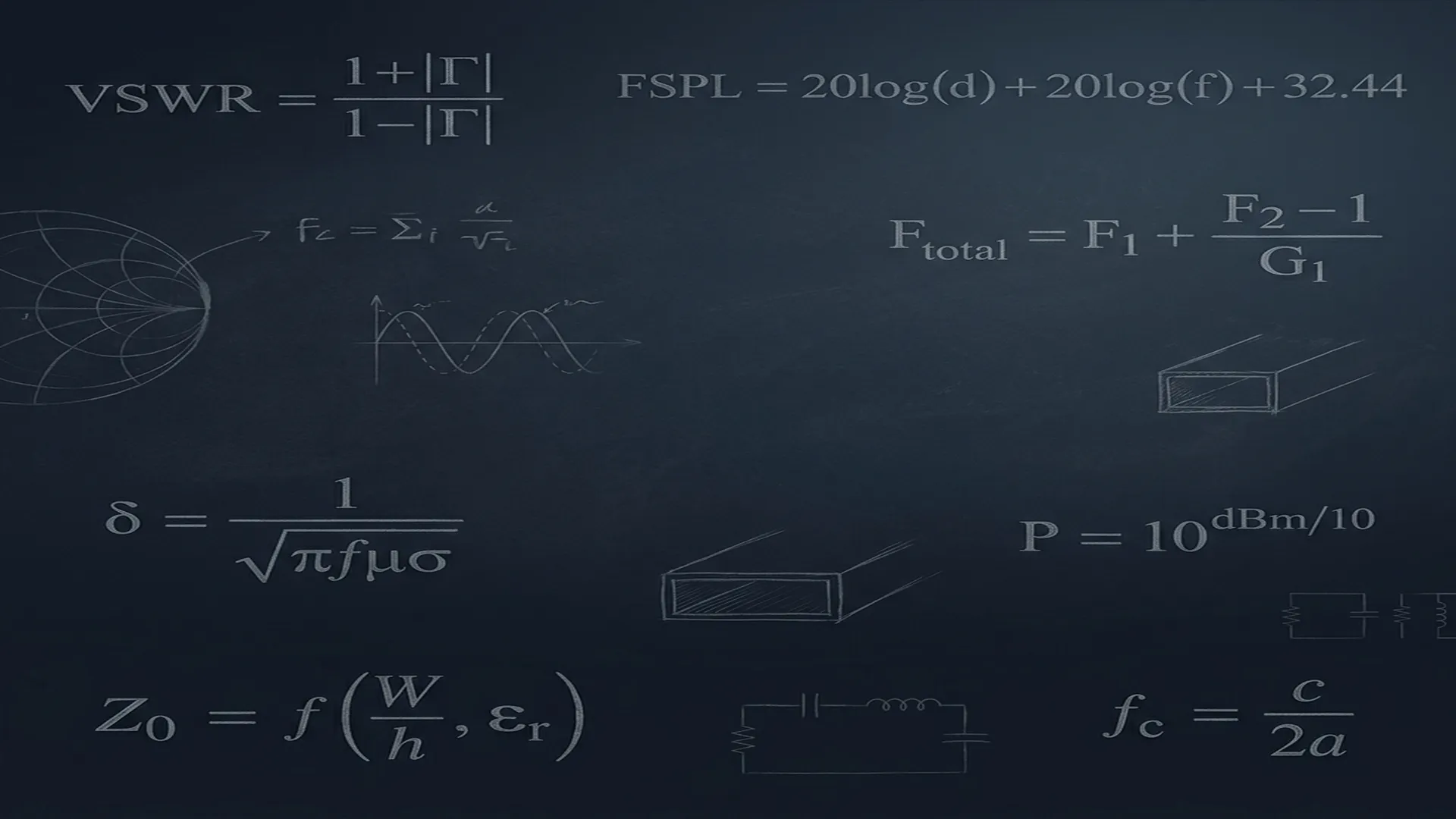
Skin Depth
Calculator
Calculate how deep current penetrates into a conductor at a given frequency. Critical for understanding conductor losses, plating thickness requirements, and waveguide performance at mmWave frequencies.
Input Parameters
Skin Depth of Copper at Common Frequencies
| Frequency | δ Copper (μm) | δ Gold (μm) | δ Silver (μm) | δ Aluminum (μm) |
|---|---|---|---|---|
| 1 MHz | 66.09 | 78.61 | 63.44 | 82.04 |
| 100 MHz | 6.61 | 7.86 | 6.34 | 8.20 |
| 1 GHz | 2.09 | 2.49 | 2.01 | 2.59 |
| 10 GHz | 0.661 | 0.786 | 0.634 | 0.820 |
| 28 GHz | 0.395 | 0.470 | 0.379 | 0.490 |
| 40 GHz | 0.331 | 0.393 | 0.317 | 0.410 |
| 60 GHz | 0.270 | 0.321 | 0.259 | 0.335 |
| 77 GHz | 0.238 | 0.283 | 0.229 | 0.296 |
| 110 GHz | 0.200 | 0.237 | 0.191 | 0.248 |
The Skin Effect in RF Engineering
At DC, current flows uniformly through the entire cross-section of a conductor. As frequency increases, electromagnetic fields within the conductor cause current to concentrate near the surface. This is the skin effect, and at RF frequencies, it means the effective conducting area is just a thin shell near the surface.
The Formula
Where:
δ = skin depth (meters)
f = frequency (Hz)
μ₀ = 4π × 10⁻⁷ H/m (permeability of free space)
σ = conductivity (S/m)
Why Skin Depth Matters for RF Design
- Conductor losses: Since current only flows in a thin surface layer, the effective resistance of an RF conductor is much higher than its DC resistance. This is why conductor losses increase with frequency.
- Plating thickness: Gold or silver plating on waveguide components only needs to be a few skin depths thick to carry RF current. Beyond 3-5 skin depths, additional plating thickness provides no RF benefit.
- Surface finish: At mmWave frequencies where skin depth is sub-micrometer, surface roughness becomes a significant factor in conductor loss. Rough surfaces force current to travel a longer path, increasing loss.
- Waveguide performance: Waveguide insertion loss is directly related to the skin depth of the wall material. Lower skin depth (higher conductivity) means lower loss.
Plating Guidelines for Waveguide Components
For waveguide and RF connectors, the recommended plating thickness is 3 to 5 skin depths at the lowest operating frequency. This ensures that the RF current sees only the plating material, not the base metal underneath.
| Waveguide Band | Freq Range | δ Gold | Min Gold Plating (3δ) | Typical Spec |
|---|---|---|---|---|
| WR-42 (Ka) | 18 – 26.5 GHz | 0.58 μm | 1.7 μm | 2 – 3 μm |
| WR-28 (Ka) | 26.5 – 40 GHz | 0.47 μm | 1.4 μm | 2 – 3 μm |
| WR-15 (V) | 50 – 75 GHz | 0.36 μm | 1.1 μm | 1.5 – 2 μm |
| WR-10 (W) | 75 – 110 GHz | 0.28 μm | 0.85 μm | 1 – 2 μm |
Frequently Asked Questions
What is skin depth?
Skin depth (δ) is the depth below a conductor's surface where current density drops to 37% (1/e) of its surface value. At 10 GHz, copper's skin depth is only 0.66 μm, meaning virtually all RF current flows in a layer less than a micrometer thick.
What is the skin depth of copper at 10 GHz?
Approximately 0.66 μm (0.026 mils). At 28 GHz it decreases to 0.39 μm, and at 77 GHz to about 0.24 μm. Skin depth decreases with the square root of frequency.
How thick should gold plating be on a waveguide?
Minimum 3-5 skin depths at the lowest operating frequency. For WR-28 (26.5-40 GHz), this means at least 1.4-2.4 μm of gold. Most manufacturers specify 2-3 μm.
Why is gold used instead of copper for waveguide plating?
Gold does not oxidize. While gold has about 70% of copper's conductivity, copper oxide is a very poor conductor that quickly degrades RF performance. Silver has the best conductivity but tarnishes. Gold provides the best long-term performance stability.