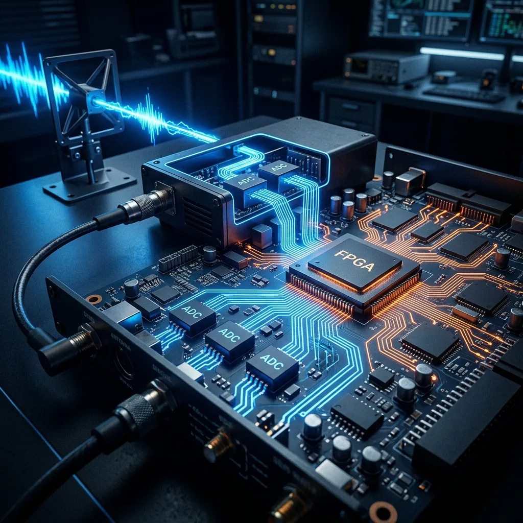
Software-defined radio has moved from academic curiosity to operational necessity. Modern SIGINT receivers, electronic warfare systems, 5G base stations, and spectrum monitoring platforms all depend on SDR architectures that push analog-to-digital conversion as close to the antenna as possible. The result is a receiver where most of the signal processing happens in firmware, not hardware, allowing a single platform to cover multiple frequency bands, modulation schemes, and waveform standards through software changes alone.
For RF engineers, SDR is not about eliminating analog hardware. It is about understanding exactly where the boundary between analog and digital should sit for a given application, and designing the RF front end to deliver the cleanest possible signal to that boundary. This article walks through the complete SDR signal chain, from antenna port to digital baseband, and addresses the engineering tradeoffs at each stage.
The SDR Signal Chain: A Systems View
Every SDR architecture, regardless of its specific implementation, follows the same fundamental signal flow. RF energy enters the antenna, passes through analog conditioning stages, gets converted to digital samples, and is processed in a digital back end. The specifics of each stage vary enormously depending on operating frequency, instantaneous bandwidth, and dynamic range requirements.
| Stage | Function | Key Parameters |
|---|---|---|
| Antenna | RF energy capture | Gain, bandwidth, VSWR, polarization |
| RF Front End | Filtering, LNA, image rejection | Noise figure, IP3, selectivity |
| Downconversion | Frequency translation to IF or baseband | LO phase noise, conversion loss, spurious |
| IF / Baseband | Anti-alias filtering, gain control | Filter shape factor, AGC range |
| ADC | Analog-to-digital conversion | Sample rate, ENOB, SFDR, SNR |
| Digital Processing | DDC, filtering, demodulation | FPGA resources, latency, throughput |
RF Front End: Where Analog Precision Matters Most
The RF front end is the most critical analog stage in any SDR. Its job is to condition the incoming signal so that the ADC receives a clean, filtered, appropriately leveled waveform. Failures here propagate through the entire digital processing chain in ways that no amount of firmware can correct.
Low-Noise Amplifier (LNA) Selection
The LNA sets the noise floor of the entire receiver. In an SDR for spectrum monitoring applications, you might need a noise figure below 1.5 dB across a multi-octave bandwidth. For a narrowband communications receiver, a noise figure under 0.8 dB at a single band may be sufficient. The tradeoff is always between noise figure and linearity (IP3). A low-noise amplifier with poor linearity will generate intermodulation products that corrupt adjacent channels, particularly in dense signal environments.
Design Rule: The system noise figure is dominated by the first active stage. An LNA with a 1.0 dB noise figure followed by a mixer with 7 dB conversion loss yields a cascaded noise figure of approximately 1.1 dB (per Friis equation). Reversing the order, mixer first, yields a system noise figure of approximately 8 dB. The LNA must always precede lossy stages.
Filtering Strategy
Pre-selection filters before the LNA protect against out-of-band interference and prevent strong signals from driving the LNA into compression. In wideband SDR receivers covering 20 MHz to 6 GHz, switchable filter banks with overlapping passbands are common. Each filter path is optimized for a specific frequency range, balancing insertion loss against out-of-band rejection.
For mmWave SDR applications at Ka-band and above, waveguide-based filters provide superior performance. A WR-28 waveguide bandpass filter at 32 GHz can achieve insertion loss below 0.5 dB with 40+ dB of out-of-band rejection, performance that is difficult to match with planar filter topologies at these frequencies.
Downconversion Architecture
Most SDR systems use either superheterodyne (one or more IF stages) or direct conversion (zero-IF) architectures. The choice depends on the operating frequency and required instantaneous bandwidth.
| Architecture | Advantages | Disadvantages |
|---|---|---|
| Superheterodyne | Excellent selectivity, high dynamic range, proven heritage | More components, image rejection required, fixed IF bandwidth |
| Direct Conversion | Simpler architecture, wide instantaneous bandwidth, fewer filters | DC offset, I/Q imbalance, LO leakage, 1/f noise |
| Direct Sampling | No mixer, fewest analog components, maximum flexibility | Requires very high-speed ADC, power intensive, limited to lower frequencies |
Direct sampling, where the ADC digitizes the RF signal without any frequency conversion, is increasingly practical at frequencies below 6 GHz. Modern ADCs like the TI ADC12DJ3200 offer 12-bit resolution at 6.4 GSPS, enabling direct digitization of signals up to approximately 3 GHz without aliasing. At mmWave frequencies, superheterodyne conversion to a suitable IF remains the standard approach.
The ADC: Where Analog Becomes Digital
The analog-to-digital converter is the pivot point of the entire SDR architecture. Its performance defines the dynamic range, bandwidth, and sensitivity of the receiver. Selecting the right ADC requires balancing four interrelated parameters.
Sample Rate and Bandwidth
The Nyquist theorem requires the ADC sample rate to be at least twice the signal bandwidth. In practice, oversampling by a factor of 2.5x or more provides margin for anti-alias filter rolloff and improves SNR through processing gain. A 200 MHz instantaneous bandwidth requires a minimum sample rate of 500 MSPS, with 800-1000 MSPS being more typical in production designs.
Resolution vs. Speed
ADC resolution, measured in effective number of bits (ENOB), directly determines the dynamic range of the receiver. Each additional bit of ENOB provides approximately 6 dB of dynamic range. At the highest sample rates, ENOB drops due to aperture jitter, comparator metastability, and thermal noise within the ADC.
| ADC Example | Sample Rate | Resolution | ENOB (@ Nyquist) | SFDR |
|---|---|---|---|---|
| AD9213 | 10.25 GSPS | 12-bit | ~9.0 | 62 dBFS |
| ADC12DJ3200 | 6.4 GSPS | 12-bit | ~9.3 | 65 dBFS |
| AD9680 | 1.25 GSPS | 14-bit | ~11.0 | 82 dBFS |
| LTC2387-18 | 15 MSPS | 18-bit | ~16.0 | 100 dBFS |
Engineering Insight: Do not confuse ADC resolution (bit count) with ENOB. A 16-bit ADC with an ENOB of 11.5 at your operating frequency delivers the dynamic range of an ideal 11.5-bit converter, not a 16-bit one. Always design to the ENOB specification at the actual input frequency and sample rate, not the headline resolution.
Spurious-Free Dynamic Range (SFDR)
SFDR quantifies the ratio between the fundamental signal and the largest spurious component in the ADC output spectrum. In an SDR designed for spectrum monitoring, SFDR is often more important than SNR because weak signals must be detected in the presence of strong ones. An ADC with 75 dBFS of SFDR can detect a signal 75 dB below the full-scale input level without confusion from ADC-generated spurs.
Digital Back End: FPGA Processing
Once the signal is digitized, the FPGA performs the operations that traditionally required dedicated analog hardware: channelization, filtering, frequency translation, demodulation, and detection. This is where the "software-defined" part of SDR becomes real.
Digital Down Conversion (DDC)
The DDC is the first processing stage after the ADC. A numerically controlled oscillator (NCO) generates a complex sinusoid that is multiplied with the ADC output to translate the desired signal to baseband (zero frequency). The NCO frequency can be changed in a single clock cycle, allowing the receiver to retune across the digitized bandwidth with effectively zero tuning latency. This is fundamentally different from analog tuning, where synthesizer settling times of microseconds to milliseconds limit how quickly the receiver can switch frequencies.
Decimation and Channelization
After the DDC, cascaded integrator-comb (CIC) filters followed by finite impulse response (FIR) filters reduce the sample rate from the ADC clock to the minimum required for the channel bandwidth. A 1 GSPS ADC digitizing a 200 MHz band, but targeting a 25 kHz communications channel, requires total decimation by a factor of 40,000. This decimation also provides processing gain, improving the effective SNR of the narrow channel by approximately 10·log₁₀(40,000) = 46 dB.
FPGA Resource Considerations
Modern SDR designs target Xilinx Zynq UltraScale+ or Intel Agilex FPGA families, which integrate high-speed transceivers, DSP slices, and embedded ARM processors on a single die. The FPGA must handle the ADC data rate continuously without dropping samples. A 12-bit ADC at 3 GSPS produces approximately 36 Gbit/s of raw data, requiring careful interface design (typically JESD204B or JESD204C) and sufficient internal memory bandwidth for real-time processing.
Practical Design Considerations
Clock Distribution and Phase Noise
The clock that drives the ADC is the heartbeat of the SDR. Phase noise on the sampling clock directly degrades the SNR of the digitized signal, and this degradation worsens with increasing input frequency. A sampling clock with -150 dBc/Hz phase noise at 10 kHz offset is adequate for HF/VHF applications but may be insufficient for X-band or Ka-band IF digitization. Low-jitter clock sources with sub-100 fs RMS jitter are standard in high-performance SDR designs.
Power Supply Integrity
High-speed ADCs are extremely sensitive to power supply noise. Switching regulator ripple at 500 kHz can appear as spurious tones in the ADC output spectrum, degrading SFDR by 10 dB or more. Production SDR designs use dedicated linear regulators or heavily filtered switching supplies for ADC power rails, with power supply rejection ratio (PSRR) verified across the full frequency range of concern.
Thermal Management
A modern SDR board combining a high-speed ADC, FPGA, and supporting analog circuitry can dissipate 30 to 80 watts. Thermal design must account for the tight coupling between component temperature and RF performance. ADC ENOB degrades with increasing junction temperature, typically 0.1 to 0.3 bits per 10°C rise. LNA noise figure and gain also shift with temperature. Consistent thermal management is not a luxury; it is a performance requirement.
Where Waveguide Meets Software
SDR architecture discussions often focus on the digital side, but the analog front end determines what the digital system can actually achieve. No amount of FPGA processing can recover a signal that was lost to insertion loss in the RF chain, corrupted by a noisy LNA, or distorted by a poorly terminated waveguide port.
At mmWave frequencies, this connection becomes critical. An SDR receiver operating at Ka-band (26 GHz) with a waveguide front end requires every component in the analog chain, from the antenna feed to the waveguide-to-coax transition, to be specified, manufactured, and verified against tight performance budgets. A 0.3 dB increase in waveguide insertion loss at 26 GHz directly reduces the receiver's sensitivity by 0.3 dB, which is equivalent to reducing the ADC's ENOB by approximately 0.05 bits. In a link-limited system, that fraction of a dB can be the margin between detection and missed signal.
The convergence of precision RF hardware and high-performance digital processing is what makes modern SDR systems possible. The antenna, the waveguide, the LNA, the mixer, and the ADC are not independent subsystems. They are links in a chain where the weakest component defines the performance of the whole.
RF Essentials manufactures precision waveguide components, terminations, and integrated assemblies that form the analog foundation of high-performance SDR systems. All products are made in the USA.
Frequently Asked Questions
What defines a software-defined radio architecture?
It pushes analog-to-digital conversion as close to the antenna as possible so most of the signal processing happens in firmware rather than fixed hardware. That lets a single platform cover multiple frequency bands, modulation schemes, and waveform standards through software changes alone. For the RF engineer, the real task is deciding where the boundary between analog and digital should sit and designing the front end to deliver the cleanest possible signal to that boundary.
Why does the RF front end matter most in an SDR?
It conditions the incoming signal before the ADC, and any failure there propagates through the whole digital chain in ways firmware cannot fix. The first active stage dominates system noise figure, so the LNA must precede lossy stages: by the Friis equation, a 1.0 dB noise-figure LNA ahead of a 7 dB mixer gives about 1.1 dB system noise figure, while putting the mixer first gives about 8 dB. Pre-selection filters also keep strong out-of-band signals from compressing the LNA.
What downconversion architectures do SDRs use?
Superheterodyne offers excellent selectivity and dynamic range but needs image rejection and more components. Direct conversion, or zero-IF, is simpler with wide instantaneous bandwidth but suffers DC offset, I/Q imbalance, and LO leakage. Direct RF sampling skips the mixer entirely for maximum flexibility but demands a very high-speed ADC and is practical below about 6 GHz. At millimeter-wave frequencies, superheterodyne conversion to a suitable IF remains the standard approach.