An RF circuit that simulates perfectly can fail completely on a PCB. The difference between simulation and reality is the layout. Every trace is a transmission line. Every via is an inductor. Every gap in the ground plane is a slot antenna. Every unshielded trace is a potential coupling path. RF PCB layout is not about aesthetics or routing convenience. It is about controlling electromagnetic fields, maintaining impedance continuity, and preventing unintended coupling between circuits.
1. Microstrip vs. Stripline
| Property | Microstrip | Stripline |
|---|---|---|
| Structure | Trace on surface, ground below | Trace between two ground planes |
| Isolation | Moderate (fields in air) | Excellent (fields contained between grounds) |
| Loss | Lower at same frequency | Higher (more dielectric loss) |
| Component access | Easy (surface mount) | Difficult (buried trace) |
| Dispersion | Higher (inhomogeneous medium) | Lower (homogeneous medium) |
| Best for | General RF, component integration | High-isolation, multi-channel systems |
Impedance Control
The characteristic impedance of a microstrip trace depends on trace width, substrate height, substrate dielectric constant, and trace thickness. For 50 ohms on standard Rogers RO4003C (Er = 3.55, 20 mil substrate), the trace width is approximately 45 mils. Change the substrate to RO4350B (Er = 3.66), and the width changes to 43 mils. Every material and stackup combination requires its own impedance calculation.
Use an Impedance Calculator, Not Rules of Thumb: "Make the trace width equal to the substrate height" is a common approximation for 50 ohms on FR-4, but it is only roughly correct and fails for high-frequency substrates. Use a field solver (Polar Si9000, Saturn PCB Toolkit, or your EDA tool's built-in calculator) with the actual stackup parameters from your fabricator. Request the fabricator's dielectric constant at your operating frequency, not the datasheet value at 1 MHz.
2. Ground Plane Management
Rule 1: Continuous Ground Under RF Traces
The return current for a microstrip trace flows on the ground plane directly beneath the trace. If there is a slot, split, or gap in the ground plane under the trace, the return current must flow around the gap, creating a loop antenna that radiates and picks up interference. Never route a signal trace over a ground plane split.
Rule 2: Separate Analog and Digital Grounds Carefully
In mixed-signal systems, the digital ground and analog ground should be connected at a single point near the ADC/DAC. The analog RF section should have its own continuous ground plane that is never broken by digital signal vias or power plane routing.
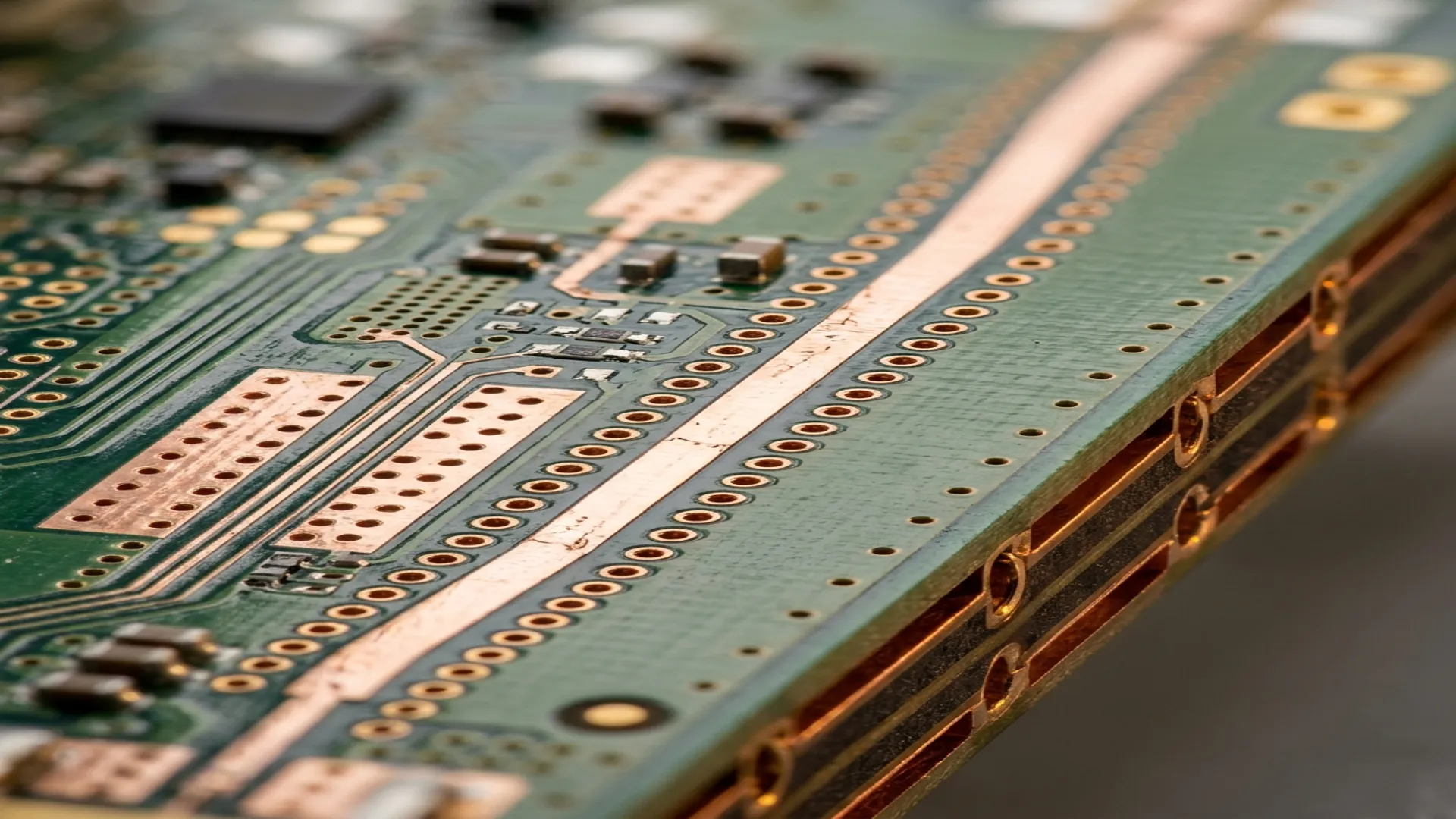
Rule 3: Ground Vias at Component Pads
Every component that connects to ground (decoupling capacitors, shunt elements in matching networks, amplifier source pins) needs ground vias immediately adjacent to the pad. "Immediately" means within 10 mils of the pad edge. The inductance of a via (approximately 0.5 to 1 nH for a standard 10-mil via through a 62-mil board) adds impedance to the ground connection. At 10 GHz, 1 nH of via inductance is 63 ohms of reactance.
3. Via Fencing
Via fencing (also called via stitching or via curtains) is a row of ground vias placed along both sides of a microstrip trace or around an RF section to contain the electromagnetic fields and prevent coupling to adjacent circuits.
Design Rules
- Via spacing: Less than lambda/20 at the highest operating frequency. At 10 GHz (lambda = 30 mm), via spacing should be less than 1.5 mm (59 mils).
- Via-to-trace distance: At least 3x the substrate height from the trace edge to the via fence edge. Closer than this, the vias perturb the trace impedance.
- Via diameter: Standard 10 to 12 mil drill. Smaller vias have higher inductance but allow tighter spacing.
- Double-row fencing: For critical isolation (adjacent transmit and receive channels), use two rows of vias with staggered spacing for improved shielding effectiveness.
4. Connector Launch Design
The transition from an SMA connector to a PCB microstrip trace is a critical impedance discontinuity. A poor connector launch can add 0.5 dB of insertion loss and degrade return loss to -10 dB at frequencies above 10 GHz.
- Ground pad continuity: The connector ground pins must connect to the PCB ground plane with multiple vias directly at the pad. No trace routing, no shared vias.
- Signal pin length: Minimize the length of the connector signal pin landing on the PCB. The exposed pin is an uncontrolled-impedance section. Shorter is better.
- Anti-pad sizing: The clearance hole in the ground plane around the signal via must be sized to maintain 50 ohms. Too large increases impedance; too small decreases it.
- Edge-launch preferred: Edge-launch (end-launch) SMA connectors provide better impedance control and lower VSWR than vertical-launch connectors at frequencies above 6 GHz.
5. Decoupling Strategy
RF amplifier and oscillator supply pins require careful decoupling to prevent RF energy from coupling onto the DC power bus:
- Capacitor selection: Use multiple capacitor values in parallel (100 pF + 1 nF + 100 nF) to cover a wide impedance bandwidth. Each capacitor has a series self-resonant frequency; the parallel combination fills the gaps.
- Placement: The smallest capacitor (highest SRF, lowest impedance at the highest frequency) goes closest to the device pin. The largest capacitor goes farthest.
- Via placement: Each decoupling capacitor needs its own dedicated ground via directly at the ground pad. Do not share ground vias between decoupling caps.
6. Common Layout Mistakes
- Trace width changes at component pads: When a 50-ohm trace meets a 0402 component pad, the pad width is different from the trace width, creating an impedance bump. Taper the trace into the pad gradually or compensate with a narrowing section.
- Right-angle bends: A 90-degree microstrip bend has excess capacitance at the corner. Use 45-degree mitered bends or curved bends (radius > 3x trace width) for controlled impedance.
- Parallel trace coupling: Two parallel microstrip traces separated by less than 3x the substrate height will couple significantly. Route RF traces with maximum separation, and use via fencing between them.
- Ignoring the board edge: Microstrip traces near the board edge lose their ground plane reference. Keep RF traces at least 5x the substrate height away from board edges.
Use our free RF calculators to verify your PCB trace impedance, VSWR, and return loss during the design phase.
Frequently Asked Questions
Why can an RF circuit that simulates perfectly fail on a PCB?
The difference between simulation and reality is the layout. On a real board every trace is a transmission line, every via is an inductor, every gap in the ground plane is a slot antenna, and every unshielded trace is a coupling path. RF PCB layout is not about routing convenience; it is about controlling electromagnetic fields, maintaining impedance continuity, and preventing unintended coupling between circuits, which is where a clean simulation goes wrong.
Why must you never route an RF trace over a ground-plane split?
The return current for a microstrip trace flows on the ground plane directly beneath it. A slot, split, or gap forces that return current to detour around the opening, forming a loop that radiates and picks up interference. Keep a continuous ground under RF traces, and place ground vias within 10 mils of every component ground pad, because a 1 nH via presents 63 ohms of reactance at 10 GHz.
What is via fencing and how should it be spaced?
Via fencing is a row of ground vias placed along both sides of a trace or around an RF section to contain the fields and prevent coupling to neighboring circuits. Spacing should be less than a twentieth of a wavelength at the top operating frequency, under about 1.5 mm at 10 GHz, and the fence should sit at least three substrate heights from the trace edge so it does not perturb the trace impedance. Double-row staggered fencing improves isolation between transmit and receive channels.