Maximum power transfer occurs when the source impedance is the complex conjugate of the load impedance. When they do not match, some portion of the signal reflects back toward the source. This reflection wastes power, degrades system noise figure, distorts amplifier linearity, and in high-power systems, can damage transmitter output stages. The impedance matching network is the circuit that transforms one impedance to another so that the source sees a matched load.
This guide covers the three fundamental matching network topologies, how to choose between them, and the practical constraints that make textbook designs fail on real PCBs.
1. The L-Network
The L-network is the simplest matching topology: two reactive elements (one series, one shunt) arranged in an L shape. It can transform any impedance to any other impedance at a single frequency.
Two Configurations
- Low-pass L (series L, shunt C): Transforms a low impedance up to a higher impedance. The series inductor adds positive reactance and the shunt capacitor provides a path to ground.
- High-pass L (series C, shunt L): Transforms a high impedance down to a lower impedance. Also provides DC blocking, which can be useful for biasing active devices.
The L-Network Limitation: An L-network has exactly one degree of freedom after you set the source and load impedances. This means you cannot independently control the Q factor (bandwidth). The Q is fixed by the impedance transformation ratio: Q = sqrt(R_high/R_low - 1). If you need to control bandwidth independently, you need a three-element network (Pi or T).
| Transform Ratio (R_high/R_low) | L-Network Q | Fractional Bandwidth | Bandwidth at 2.4 GHz |
|---|---|---|---|
| 2:1 | 1.0 | 100% | 2,400 MHz |
| 4:1 | 1.73 | 58% | 1,390 MHz |
| 10:1 | 3.0 | 33% | 800 MHz |
| 50:1 | 7.0 | 14% | 340 MHz |
2. The Pi-Network
The Pi-network uses three reactive elements: two shunt elements and one series element, forming the shape of the Greek letter Pi. It is equivalent to two cascaded L-networks with a virtual intermediate impedance.
Why Use Pi
- Independent Q control: The virtual intermediate impedance is a free variable. By choosing it lower than both the source and load impedance, you increase the Q. By choosing it only slightly lower, you decrease the Q. This gives you direct control over the bandwidth of the match.
- Harmonic suppression: The low-pass Pi-network (shunt C, series L, shunt C) naturally attenuates harmonics because of its filter-like frequency response. This makes it the standard topology for power amplifier output matching where harmonic rejection is critical.
- Practical component values: The shunt capacitors in a Pi-network can absorb parasitic capacitances from the PCB pads, connectors, and device packages.
3. The T-Network
The T-network is the dual of the Pi: two series elements and one shunt element. It is less common than the Pi for power applications but has specific advantages:
- High-Q matching: The T-network naturally produces higher Q (narrower bandwidth) than a Pi for the same impedance transformation. Useful for narrowband filter-matching combinations.
- Series inductors for DC feed: The two series inductors in a low-pass T-network can double as DC bias chokes, simplifying the bias network in amplifier designs.
- Caution: The T-network's virtual intermediate impedance is higher than both source and load, which means higher circulating currents and higher component stress. Not ideal for high-power applications.
| Topology | Elements | Q Control | Best For | Harmonic Rejection |
|---|---|---|---|---|
| L-Network | 2 | No (fixed by ratio) | Simple, wideband matches | Minimal |
| Pi-Network | 3 | Yes (adjustable) | PA output, harmonic filtering | Good (low-pass form) |
| T-Network | 3 | Yes (adjustable) | Narrowband, bias integration | Poor (high-pass form) |
4. Smith Chart Matching
The Smith chart is the standard tool for visualizing and designing matching networks. Each matching element traces a specific path on the chart:
- Series inductor: Moves clockwise along a constant-resistance circle (adds positive reactance).
- Series capacitor: Moves counter-clockwise along a constant-resistance circle (adds negative reactance).
- Shunt capacitor: Moves clockwise along a constant-conductance circle (adds positive susceptance).
- Shunt inductor: Moves counter-clockwise along a constant-conductance circle (adds negative susceptance).
The matching design process: plot the load impedance on the Smith chart, then apply series and shunt elements in sequence, tracing the impedance trajectory toward the center (50 ohms). The choice of path determines the topology, bandwidth, and component values.
5. Lumped vs. Distributed Elements
At frequencies below approximately 3 GHz, lumped elements (chip inductors, chip capacitors) are practical. Above 3 GHz, the self-resonant frequencies of lumped components become a limiting factor, and distributed elements (transmission line stubs, coupled lines, microstrip) become necessary.
- Below 1 GHz: Lumped elements are standard. Component parasitics are manageable with careful layout.
- 1 to 6 GHz: Transition zone. Both lumped and distributed approaches work. Lumped elements are smaller; distributed elements are more predictable.
- Above 6 GHz: Distributed elements dominate. Matching is achieved with transmission line sections, stubs, and waveguide transformers (tapered sections, stepped impedance transformers).
6. Practical Pitfalls
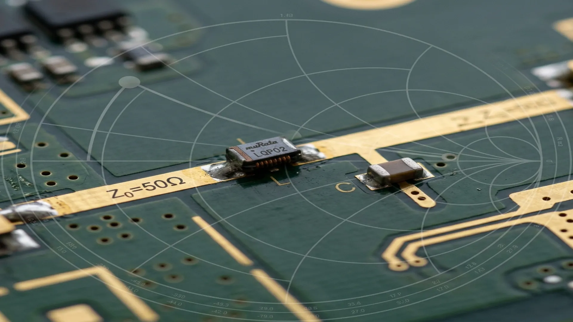
- Component parasitics: A "100 nH" chip inductor is not 100 nH at 2.4 GHz. It has parasitic capacitance, series resistance, and a self-resonant frequency. Always use the manufacturer's S-parameter model, not the nominal value.
- PCB parasitics: Every pad, via, and trace on the PCB adds parasitic inductance and capacitance. A 0402 capacitor pad adds approximately 0.1 pF of parasitic capacitance. At 5 GHz, that matters.
- Temperature drift: NP0/C0G capacitors have near-zero temperature coefficient. X7R and X5R capacitors drift significantly with temperature. Use NP0 for matching networks.
- Tolerance stacking: A matching network designed for exact component values will not produce the exact designed match when built with ±5% tolerance components. Always simulate the match with Monte Carlo analysis using realistic tolerances.
Use our free VSWR Calculator to verify your impedance match. Convert between reflection coefficient, return loss, VSWR, and mismatch loss instantly.
Frequently Asked Questions
Why does impedance matching matter?
Maximum power transfer occurs when the source impedance is the complex conjugate of the load. When they do not match, part of the signal reflects back toward the source, which wastes power, degrades system noise figure, distorts amplifier linearity, and in high-power systems can damage transmitter output stages. A matching network is the circuit that transforms one impedance into another so the source sees a properly matched load.
What is the limitation of an L-network, and when do I need a Pi or T?
An L-network of two reactive elements can transform any impedance to any other at a single frequency, but it has only one degree of freedom once the source and load are set, so its Q, and therefore its bandwidth, is fixed by the transformation ratio, the square root of R-high over R-low minus one. When you need to set bandwidth independently, you move to a three-element Pi or T network, whose virtual intermediate impedance becomes a free variable.
When should I use a Pi-network versus a T-network?
The Pi-network, two shunt elements around one series element, gives independent Q control, naturally suppresses harmonics in its low-pass form, and lets its shunt capacitors absorb device and PCB parasitics, which makes it the standard for power amplifier output matching. The T-network, two series elements around one shunt, suits narrowband matching and lets its series inductors double as DC bias chokes, but its higher intermediate impedance raises circulating currents and component stress, so it is poor for high power.