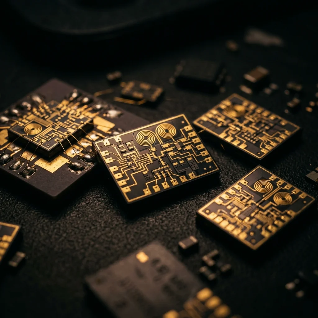
MMIC Technology
The definitive engineering resource for Monolithic Microwave Integrated Circuits. From fundamental principles to advanced design, fabrication, and system integration across DC to 300 GHz.
What Is an MMIC?
A Monolithic Microwave Integrated Circuit (MMIC) is a type of integrated circuit designed to operate at microwave and millimeter-wave frequencies, typically from 300 MHz to beyond 300 GHz. The term "monolithic" comes from the Greek monolithos (single stone), indicating that all active and passive circuit elements are fabricated on a single semiconductor substrate.
Unlike conventional silicon ICs used in digital electronics, MMICs are built on compound semiconductor substrates such as gallium arsenide (GaAs), gallium nitride (GaN), or indium phosphide (InP). These materials have superior electron mobility and higher breakdown voltages compared to silicon, enabling operation at microwave frequencies with lower noise and higher power.
A Brief History
The concept of integrating microwave circuits on a single substrate was first proposed by researchers at Texas Instruments in 1965. The first practical GaAs MMICs were demonstrated at Raytheon in the late 1970s under DARPA's MMIC program. By the 1980s, foundry processes had matured enough for military applications. The 1990s brought commercial GaAs processes for wireless communications, and the 2000s saw the rise of GaN for high-power applications and InP for terahertz frequencies.
Why Not Silicon?
Silicon dominates digital electronics, but compound semiconductors outperform silicon at microwave frequencies for several reasons:
- Higher electron mobility: GaAs has ~6x the electron mobility of silicon, enabling faster switching and lower noise at high frequencies
- Semi-insulating substrate: GaAs and InP substrates are naturally semi-insulating, providing low-loss signal paths without the parasitic substrate coupling that plagues silicon RF circuits
- Higher breakdown voltage: GaN's wide bandgap (3.4 eV) enables breakdown voltages 10x higher than GaAs, supporting high-power operation
- Direct bandgap: Compound semiconductors enable efficient photonic integration, not possible with silicon's indirect bandgap
How MMICs Work
An MMIC functions by integrating active devices (transistors) with passive elements (resistors, capacitors, inductors, and transmission lines) on a single semiconductor chip. The chip is typically 50-100 μm thick, and circuits are patterned on the top surface using photolithography.
Active Devices
The transistor is the core active element. MMIC transistor technologies include:
- pHEMT (pseudomorphic High Electron Mobility Transistor): The workhorse of GaAs MMICs. Uses a 2D electron gas (2DEG) at a heterojunction to achieve high mobility and low noise. Typical gate lengths are 0.15-0.25 μm.
- mHEMT (metamorphic HEMT): Extends pHEMT performance by growing InGaAs channels with higher indium content on GaAs substrates, bridging the gap between GaAs and InP technologies.
- GaN HEMT: High-power transistor with power densities of 5-10 W/mm, typically on SiC substrates for thermal management. Used in power amplifiers and radar transmitters.
- InP HEMT: The highest-frequency transistor technology, with fT exceeding 700 GHz. Used for terahertz and sub-millimeter wave applications.
- HBT (Heterojunction Bipolar Transistor): Used in GaAs and InP for oscillators and power amplifiers where high linearity and high current density are needed.
Passive Elements
MMIC passive components are fabricated using thin-film and thick-film processes:
- Microstrip and coplanar waveguide (CPW): Transmission lines formed by patterned metal on the substrate surface. Microstrip uses a ground plane on the back side; CPW keeps all conductors on one side.
- MIM capacitors: Metal-Insulator-Metal capacitors using silicon nitride (Si3N4) dielectric, typically 200-400 pF/mm².
- Spiral inductors: Planar spiral coils providing 0.1-10 nH inductance. Quality factor (Q) is critical for filter and matching network performance.
- Thin-film resistors: NiCr or TaN resistive layers providing 50-100 Ω/square sheet resistance.
- Via holes: Etched through the substrate to connect the top-side circuit to the backside ground plane, critical for grounding and thermal management.
MMIC Substrate Materials
The choice of semiconductor substrate determines an MMIC's frequency range, power capability, noise performance, and cost. Each material has distinct physical properties that make it suitable for specific applications.
| Property | GaAs | GaN-on-SiC | InP | SiGe BiCMOS | Si CMOS |
|---|---|---|---|---|---|
| Bandgap (eV) | 1.42 | 3.40 | 1.35 | ~1.1 | 1.12 |
| Electron Mobility (cm²/Vs) | 8,500 | 2,000 | 12,000 | ~4,500 | 1,400 |
| Breakdown Field (V/cm) | 4×10&sup5; | 3.3×10&sup6; | 5×10&sup5; | 3×10&sup5; | 3×10&sup5; |
| Thermal Conductivity (W/mK) | 46 | 490 (SiC) | 68 | 130 | 150 |
| Max Frequency (GHz) | ~110 | ~100 | >300 | ~120 | ~60 |
| Power Density (W/mm) | 0.5-1 | 5-10 | 0.3-0.5 | ~0.3 | <0.1 |
| Noise Figure | Excellent | Good | Best | Good | Fair |
| Substrate Type | Semi-insulating | SiC (conductive) | Semi-insulating | Si (lossy) | Si (lossy) |
| Relative Cost | Medium | High | High | Low | Lowest |
| Primary Use | LNAs, switches, mixers | Power amps, radar TX | THz, ultra-low noise | 5G, automotive | Consumer WiFi |
GaAs (Gallium Arsenide)
The most mature and widely used MMIC substrate. GaAs pHEMT processes with 0.15 μm gate lengths are the industry standard for low-noise amplifiers, switches, mixers, and attenuators from DC to 110 GHz. The semi-insulating substrate provides naturally low-loss signal routing, and decades of process development have made GaAs the most cost-effective compound semiconductor for moderate volumes. Multiple foundries offer multi-project wafer (MPW) runs, making GaAs accessible for prototyping.
GaN (Gallium Nitride on SiC)
GaN's wide bandgap (3.4 eV) enables 5-10x higher power density than GaAs, with breakdown voltages exceeding 100V. When grown on silicon carbide (SiC) substrates, GaN benefits from SiC's exceptional thermal conductivity (490 W/mK), allowing efficient heat removal at high power levels. GaN MMICs dominate military radar transmitters, electronic warfare systems, 5G base station power amplifiers, and satellite communication uplinks. GaN-on-Si is emerging as a lower-cost alternative for applications where thermal performance is less critical.
InP (Indium Phosphide)
InP offers the highest electron mobility and the highest transistor cutoff frequencies (fT > 700 GHz) of any MMIC technology. InP HEMTs and InP HBTs enable circuits operating above 300 GHz, into the terahertz range. InP also provides the lowest noise figures at millimeter-wave frequencies, making it the preferred technology for radio astronomy receivers, deep-space communication, and security imaging systems. InP substrate costs are higher than GaAs, limiting its use to performance-critical applications.
SiGe BiCMOS
SiGe adds germanium to silicon transistors, creating a heterojunction that boosts fT to 300+ GHz while remaining compatible with standard silicon CMOS foundries. SiGe BiCMOS offers the best cost-performance tradeoff for high-volume applications up to ~100 GHz, including 5G phased arrays, automotive radar (77 GHz), and fiber-optic transceivers. The ability to integrate analog RF circuits with digital logic on the same die is a unique advantage over compound semiconductor processes.
MMIC Component Types
MMICs serve every function in a microwave signal chain. Each component type is optimized for specific performance parameters.
Freq: DC to 300 GHz | Substrate: GaAs, InP
Freq: DC to 100 GHz | Substrate: GaN, GaAs
Types: Single, double, triple balanced; I/Q
Speed: 2-10 ns | Substrate: GaAs
Tuning: 5-30% | Substrate: GaAs, SiGe
RMS Error: <5° | Substrate: GaAs, SiGe
Accuracy: ±0.2 dB | Substrate: GaAs
Freq: Up to 300+ GHz | Substrate: GaAs, InP
MMIC Fabrication Process
MMIC fabrication is a multi-step cleanroom process that patterns active and passive components on a semiconductor wafer. A typical GaAs pHEMT process involves 15-25 mask layers and takes 8-12 weeks from wafer start to completion.
MMIC vs. Hybrid MIC
The fundamental choice in microwave circuit realization: monolithic integration on semiconductor, or hybrid assembly of discrete components on a passive substrate. Each approach has distinct advantages.
- + All components on one die
- + Smallest size and weight
- + Excellent unit-to-unit repeatability
- + Low cost at high volume
- + No wire bonds between components
- + Highest frequency capability
- + Best for phased array elements
- − High NRE (mask set + foundry run)
- − No post-fab tuning
- − Limited component value range
- + Lower NRE, faster prototyping
- + Post-assembly tuning possible
- + Mix best-in-class discrete components
- + Higher power handling per assembly
- + Flexible substrate choice (alumina, LTCC)
- + Practical for low volumes
- + Wider component value range
- − Larger size and weight
- − Wire bond parasitics limit frequency
- − Unit-to-unit variation
MMIC Design Considerations
Designing an MMIC requires balancing electrical performance, physical layout, thermal management, and manufacturability. Here are the critical factors that influence a successful MMIC design.
Impedance Matching
Most MMIC circuits are designed for 50 Ω input/output impedance to interface with standard test equipment and system components. Matching networks use transmission line stubs, spiral inductors, and MIM capacitors. At millimeter-wave frequencies, distributed (transmission line) matching is preferred over lumped elements because inductor Q degrades and parasitic capacitance dominates. Multi-section matching networks trade bandwidth for loss.
Stability
Amplifier stability (K-factor > 1 at all frequencies) is non-negotiable. Resistive loading, source degeneration inductance, and odd-mode stabilization resistors between parallel transistor cells are standard techniques. Stability must be guaranteed from DC through the transistor's fmax, not just the operating band.
Thermal Management
Power MMICs must dissipate significant heat. Via holes under transistor source fingers provide the primary thermal path to the backside ground. GaN-on-SiC benefits from SiC's 490 W/mK thermal conductivity. Die attach material (AuSn solder or conductive epoxy), carrier material, and heatsink design complete the thermal stack. Junction temperature must stay below the reliability limit (typically 175-200°C for GaAs, 225-275°C for GaN).
Electromagnetic Simulation
All MMIC layouts require full-wave electromagnetic simulation (typically using tools like Momentum, Sonnet, or HFSS) to capture coupling between adjacent transmission lines, discontinuity effects at bends and junctions, and substrate mode excitation. Schematic-level simulation alone is insufficient for frequencies above ~20 GHz.
Design Rule Compliance
Every foundry provides a Process Design Kit (PDK) with design rules: minimum gate-to-gate spacing, metal width/spacing, via hole placement, MIM capacitor area limits, and edge exclusion zones. DRC (Design Rule Check) and LVS (Layout vs. Schematic) verification are mandatory before tapeout.
Yield and Testability
MMIC yield depends on die area, process defect density, and design margins. Smaller die have higher yield. On-wafer test structures (PCMs) on every wafer monitor process parameters. RF probe pads in the MMIC layout enable on-wafer testing before dicing, critical for known-good-die (KGD) programs.
Where MMICs Are Used
MMICs are critical components in virtually every modern RF and microwave system. Their combination of small size, high performance, and repeatability makes them indispensable across industries.
Frequently Asked Questions
What is an MMIC?
A Monolithic Microwave Integrated Circuit (MMIC) is an integrated circuit that operates at microwave and millimeter-wave frequencies (300 MHz to 300+ GHz). All components, including transistors, resistors, capacitors, inductors, and transmission lines, are fabricated on a single semiconductor substrate such as GaAs, GaN, or InP.
What does "monolithic" mean?
"Monolithic" means "single stone." In MMIC context, it indicates that the entire circuit, both active and passive elements, is built on one piece of semiconductor material. This contrasts with hybrid MIC, where discrete components are mounted on a passive substrate.
What is the difference between MMIC and hybrid MIC?
In a hybrid MIC, individual transistors and passive components are assembled onto a ceramic substrate and interconnected with wire bonds. In an MMIC, everything is fabricated directly on the semiconductor wafer. MMICs are smaller, more repeatable, and cost-effective at volume. Hybrids offer more flexibility and lower NRE costs.
Which is better: GaAs or GaN?
It depends on the application. GaAs excels at low-noise receiver functions (LNAs, switches, mixers) across DC to 110 GHz. GaN is superior for high-power transmit applications (PAs, radar) due to 5-10x higher power density. Most modern T/R modules use GaN for transmit and GaAs for receive.
What frequency range do MMICs cover?
MMICs operate from below 1 GHz to above 300 GHz. GaAs and GaN cover DC to ~100-110 GHz. InP extends beyond 300 GHz. SiGe BiCMOS reaches ~120 GHz. The upper limit is set by the transistor's fT and fmax.
How much does an MMIC cost?
Unit cost depends heavily on die area, substrate material, and volume. A small GaAs MMIC die (1-2 mm²) in production volume can cost $1-10 each. Large GaN PAs may cost $50-500+. NRE for a new MMIC design (mask set + foundry run) typically ranges from $50K to $500K+.
Can I prototype an MMIC?
Yes. Multi-project wafer (MPW) services allow sharing wafer space with other designs, reducing NRE to $10K-50K. Major foundries (WIN Semiconductors, UMS, OMMIC, Qorvo) offer scheduled MPW runs. SiGe foundries (GlobalFoundries, IHP, Tower) offer even lower-cost prototyping.
What tools are used for MMIC design?
Standard EDA tools include Keysight ADS (Advanced Design System) and Cadence AWR Microwave Office for circuit simulation and layout. Full-wave EM simulators (Keysight Momentum, Sonnet, Ansys HFSS) verify passive structures. Foundries provide Process Design Kits (PDKs) with calibrated device models.
MMIC Engineering Resources
Our growing library of MMIC-specific technical content. Each resource dives deep into a specific aspect of MMIC technology.