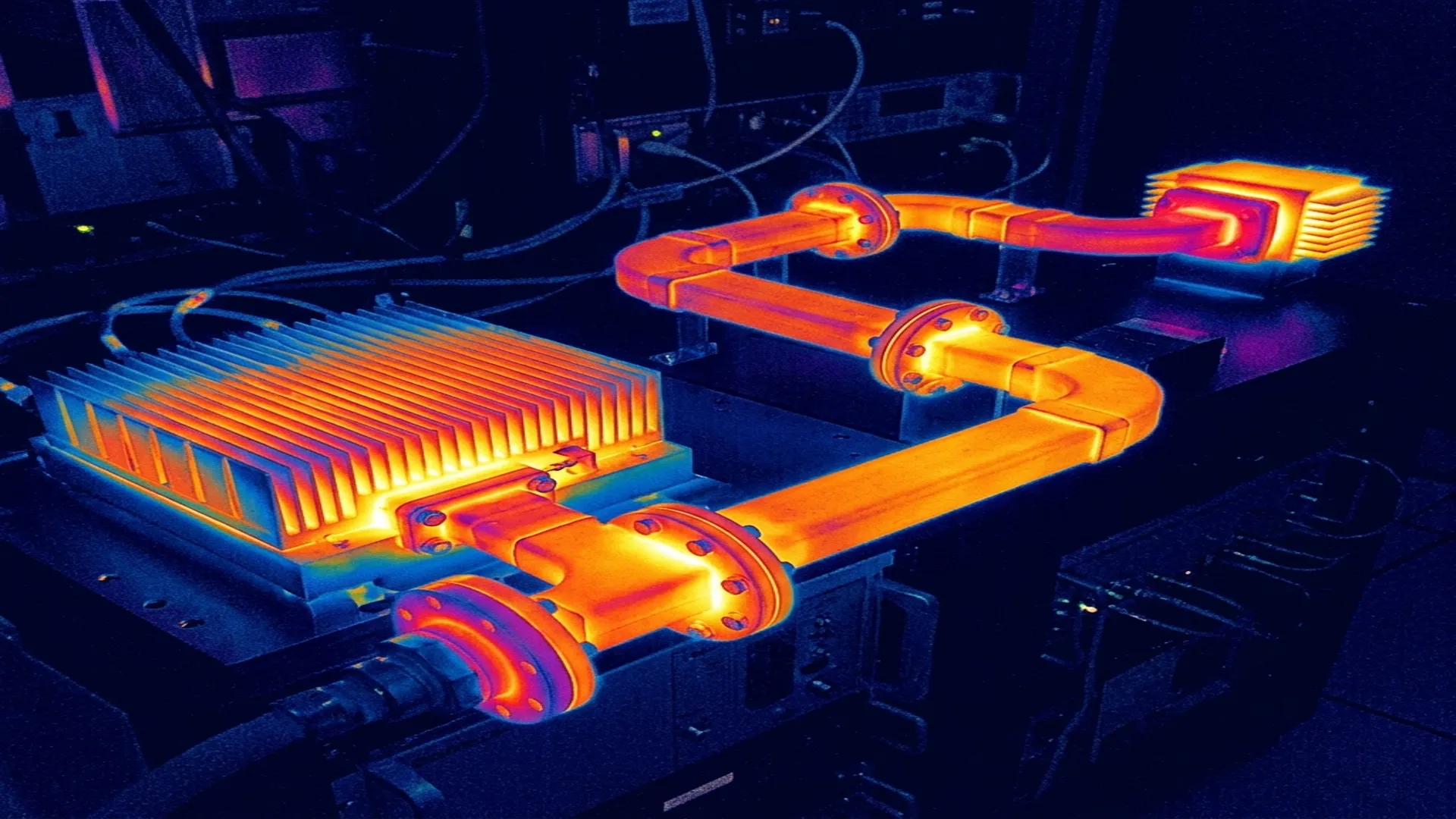
The transition from GaAs to GaN power amplifiers has changed the thermal equation for every waveguide system downstream of the PA. A GaN amplifier producing 200W in a Ka-band module concentrates that power in a smaller footprint than its GaAs predecessor. The waveguide termination absorbing that power, the coupler sampling it, and the circulator routing it must all dissipate more heat from a smaller surface area. Thermal management is no longer an afterthought in waveguide system design. It is a primary design constraint.
This application note provides the thermal calculations, derating procedures, and heat sink sizing guidelines needed to design waveguide systems that operate reliably at high power levels across the full ambient temperature range.
1. The Thermal Model
Every waveguide component that absorbs, reflects, or dissipates RF power generates heat. The thermal path from the heat source to the ambient environment can be modeled as a series of thermal resistances, analogous to electrical resistance in a circuit:
Tjunction = Tambient + Pdissipated × (θabsorber + θhousing + θinterface + θheatsink)
Where θ is thermal resistance in °C/W. The goal is to keep Tjunction below the maximum operating temperature of the absorber material (typically 150°C for carbon-loaded epoxy, 200°C for ceramic absorbers).
2. Power Derating
Component datasheets specify power handling at 25°C ambient with a defined heat sink. In real installations, the ambient temperature is higher, the heat sink may be smaller, and airflow may be restricted. The derating calculation accounts for these differences.
| Ambient Temperature | Derating Factor | Effective Power (100W rated) |
|---|---|---|
| 25°C (reference) | 1.00 | 100 W |
| 35°C | 0.80 | 80 W |
| 45°C | 0.60 | 60 W |
| 55°C | 0.40 | 40 W |
| 65°C | 0.20 | 20 W |
| 71°C (max for 150°C absorber) | 0.00 | 0 W |
The derating is linear from the reference temperature to the maximum absorber temperature. The formula is:
Pderated = Prated × (Tmax,absorber - Tambient) / (Tmax,absorber - Treference)
3. Duty Cycle and Average Power
Pulsed systems (radar, EW) generate less average heat than CW systems at the same peak power. The average power determines the thermal load:
Paverage = Ppeak × Duty Cycle
| System Type | Typical Duty Cycle | Peak Power | Average Power (Thermal Load) |
|---|---|---|---|
| Search radar | 0.1% to 1% | 10 kW | 10 to 100 W |
| Tracking radar | 5% to 25% | 1 kW | 50 to 250 W |
| Communications (CW) | 100% | 100 W | 100 W |
| EW jammer | 10% to 50% | 500 W | 50 to 250 W |
4. Heat Sink Sizing
For natural convection (no fan) in an enclosed environment, use this guideline to size the heat sink:
- Required thermal resistance: θheatsink = (Tmax,surface - Tambient) / Pdissipated - θcomponent
- Rule of thumb: For natural convection, a finned aluminum heat sink provides approximately 1°C/W per 100 cm² of total fin surface area.
- Forced air: Adding a fan reduces the heat sink thermal resistance by a factor of 3 to 5 compared to natural convection, allowing proportionally smaller heat sinks.
Material Selection
| Material | Thermal Conductivity (W/m·K) | Density (g/cm³) | Typical Use |
|---|---|---|---|
| Aluminum 6061-T6 | 167 | 2.70 | Standard heat sinks, waveguide housings |
| Copper C110 | 391 | 8.96 | High-power heat spreaders, cold plates |
| Aluminum nitride (AlN) | 170 | 3.26 | Ceramic substrates, isolating mounts |
5. Thermal Interface Materials (TIMs)
The thermal resistance of the interface between the waveguide component and the heat sink is often the dominant resistance in the thermal path. Air gaps as small as 0.001" can double the thermal resistance of the joint. Thermal interface materials fill these gaps:
- Thermal grease (silicone-based): Lowest thermal resistance (0.5 to 2.0°C·in²/W). Messy, but the best thermal performance. Use for lab and permanent installations.
- Thermal pads (silicone or graphite): Moderate thermal resistance (2.0 to 5.0°C·in²/W). Clean, easy to install, reusable. Good for field-serviceable systems.
- Indium foil: Excellent thermal performance (0.3 to 1.0°C·in²/W) and conforms to surface irregularities. Used in aerospace and military systems. Expensive.
6. System-Level Thermal Design Checklist
- Calculate average dissipated power for each component in the waveguide chain (terminations, couplers, circulators, isolators).
- Determine the worst-case ambient temperature for the installation environment.
- Apply the derating formula to verify each component can handle its power load at the worst-case ambient.
- Size the heat sink to maintain component surface temperatures below rated maximums with appropriate margin (typically 20°C margin).
- Select a thermal interface material appropriate for the thermal resistance budget and serviceability requirements.
- Verify airflow: If natural convection is insufficient, size a fan to provide the required CFM across the heat sink fins.
- Document and test: Measure actual surface temperatures with thermocouples during system integration testing to verify the thermal design.
RF Essentials manufactures high-power waveguide terminations, couplers, and assemblies with integrated heat sinking and full thermal characterization data. All products are made in the USA with power handling tested and documented.
Frequently Asked Questions
Why has the move from GaAs to GaN made waveguide thermal design harder?
GaN power amplifiers pack far more power into a smaller footprint, so a GaN module producing 200 W at Ka-band concentrates heat that the downstream termination, coupler, and circulator must shed from a smaller surface area. Thermal management has shifted from an afterthought to a primary design constraint, and components now need explicit derating, heat sinking, and interface-material choices to stay below their absorber temperature limits.
How do I derate a waveguide component for high ambient temperature?
Datasheet power handling assumes 25 C ambient, but real installations run hotter. Derating is linear between the reference and the absorber's maximum temperature: P_derated equals P_rated times (T_max minus T_ambient) divided by (T_max minus T_reference). For a 100 W part with a 150 C absorber, that leaves about 80 W at 35 C, 60 W at 45 C, and zero at 71 C. Always size for the worst-case ambient.
How does duty cycle affect the thermal load in a pulsed system?
Only average power heats the component, and average power equals peak power times duty cycle. A search radar running 0.1 to 1 percent duty at 10 kW peak dissipates just 10 to 100 W, while a 100 W CW communications link dissipates the full 100 W continuously. This is why a high peak-power radar termination can run cooler than a modest CW load, and why thermal sizing must use average, not peak, power.